- info@uenergysolar.com
- +92 42 35312001
It is the Photovoltaic cells in the Solar PV panels that convert light into electricity.
They are made from silicon layers which have had a few different chemicals added to them. These 'doping' materials mean that the cells are free enough from their orbits to ensure a DC (Direct Current) can be generated. The doped silicon is vital to all current cells, but they are made in such a way that they give polycrystalline, monocrystalline or hybrid panels. The first two of those are the most cost effective option, although the hybrid offering is what provides the most energy. All PV cells work due to light as opposed to heat, so there is no need to worry about functionality being lessened in winter or overcast months due to the colder weather; the main factors are the amount of time it is light in the day and/or the angle of the sun.
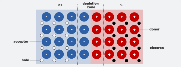
When un-doped, semiconductors are a 'halfway house' between insulators and conductors. These form a lattice, in which every electron has a particular location. Most of these have four 'valence' electrons, which are electrons in the outer shell. Electrical behaviour can thus be changed by adding in 1-2% of atoms with five valence electrons such as Phosphorus. However, there aren't enough Phosphorus atoms added to affect the structure of the entire crystal, although the fifth atom doesn't easily fit in the pattern, and is consequently knocked loose. It's then knocked through the bulk material, and this is known as a negative (n-type) semiconductor. A semiconductor can also be doped by a three-electroned atom, for example boron, which has the opposite effect, and means the structure is now minus an electron, called a hole. This on the other hand is a positive (p-type) semiconductor.![]()
A diode is created when a hole-doped semiconductor is put with an electron-doped semiconductor, and other combinations can create other devices, such as transistors.
When the two types are put together, a p-n junction is formed, as the excess electrons of the n-type atoms go to the p-type atom, and both leave exposed charges on doped atom sites, which are fixed within the structure of the crystal. The zone in between the junction is therefore named the 'depletion zone,' as there is no charge in that area.
What happens next in the process, is when light from a suitable wavelength hits the p-n junction and gets soaked up, energy is transferred to some of the electrons on the material. These then create an electrical current by flowing through the aforementioned 'depletion zone.'
A metallic contact is placed on top of the PV cells, which allows the current to flow out of the semiconductor, with the 'holes' moving in the opposite direction to the bottom of the cell until they hit a metallic contact at the bottom of the cell which means they then get filled with electrons from the other half of the circuit. A direct current (DC) is then created, which an inverter converts into usable alternating current (AC) energy. PV cells have no moving parts, and consequently have a lifespan of at least forty years.
When the model is providing its maximum power output, usually under conditions with a clear sky, strong sunlight and little shading, this is known as the Peak Power (Wp). It can also be described as peak watts/wattage, and is worked out through the electrical output in watts under the regular testing conditions of 1000W/m² of solar insolation, 25ºC and a particular solar spectrum which is described as AM (Air Mass) 1.5.
Upon the manufacturing of all the cells, they are then placed on an aluminium panel, with a reflective back coating, anti-reflective front coating and toughened low-iron glass, in order to maximise the absorption of light.
DO not miss any new information.
© 2020 U Energy Solar Pakistan. All rights reserved | Design by U Energy Solar